
Over the years that I’ve made PCBs, I’ve used two main fab houses, APC and Advanced Circuits. For a while, I’ve been hearing some good things about OSH Park so I decided to give them a try for my latest project (which I will be talking about in a later post!). For those of you not in the know, OSH Park is a company that takes in gerber files from people who want their boards fabricated, panelizes those boards into one big board then ships it off to a fab house. Once the panels are made, each individual boards are cut out and sent to their respective customers.
There were three big things about OSH Park that made me want to try them out. First, their price point was great. At $5 per square inch and you get three boards? How could I say no? Second, the boards had an ENIG finish. I prefer ENIG to HASL finishes because they look nice and they are much more resistant to corrosion. Finally, OSH Park boards had purple soldermask, a nice departure from standard, boring green masks (although many fab houses offer other colours!).
The Boards
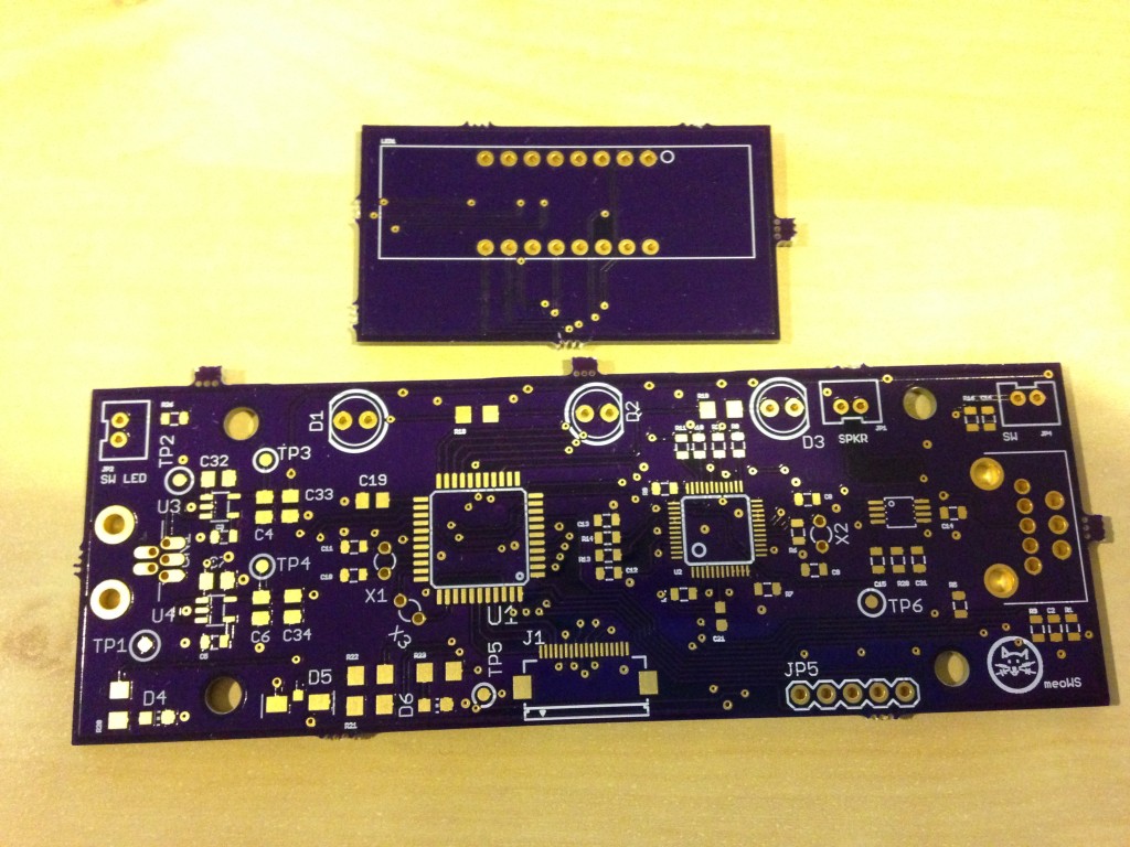
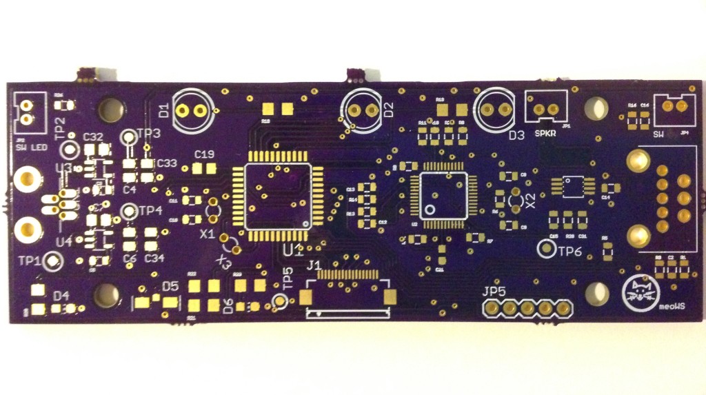
I had two kinds of boards made at OSH Park. The larger board (the main board) is your standard mix of thru-hole and surface mount components. Nothing fancy. The other board houses a seven segment display, some resistors and a FFC connector.
Good Points
At first glance, the boards looked quite nice. The combination of the gold finish and purple solder mask was especially a nice touch. There were no traces of un-etched copper, shorting lines and there were no signs of over-etching – although I could have increased the width of some of the thru-hole pads to avoid the possibly of breakout should there have been over-etching present. From the top, the holes looked well-aligned and the solder mask/artwork were where they should be. From the top, the board was quite well made. Looking at the bottom of the board however, revealed a few not-so-great things.
Bad Points
While from the top side, the holes were well-aligned, the same couldn’t have been said for the bottom side.
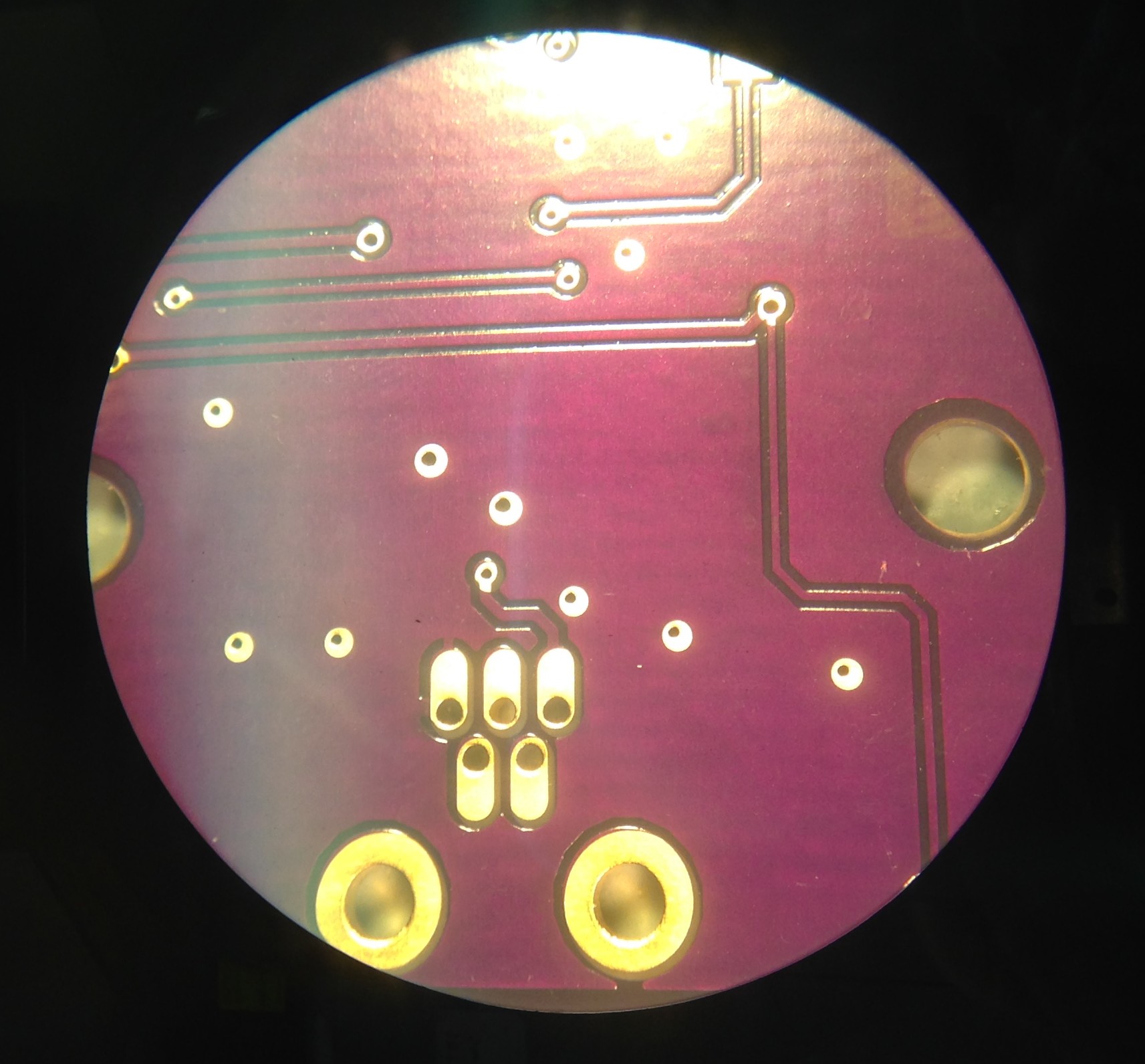
The picture on the right shows that a lot of the holes were off-center, whereas their top counterparts were centered. I’ve noticed this with pretty much all of the vias on the bottom side. It seems as if there was some sort of offset when etching away the bottom side. It also looks like some of the holes are close to breakout. Fortunately, none actually did.
The next picture shows the same off-center drills but notice the via near the top of the photo underneath the two holes spaced 0.1″ apart. Some of the via’s pad is covered by solder mask (which, itself seems to be misaligned and many other vias also got partially covered) and is dangerously close to touching the trace directly below it. This happens with another via just to the right of the via under question.
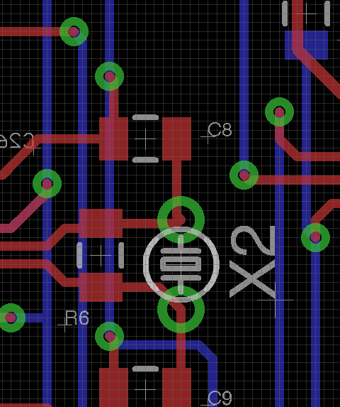
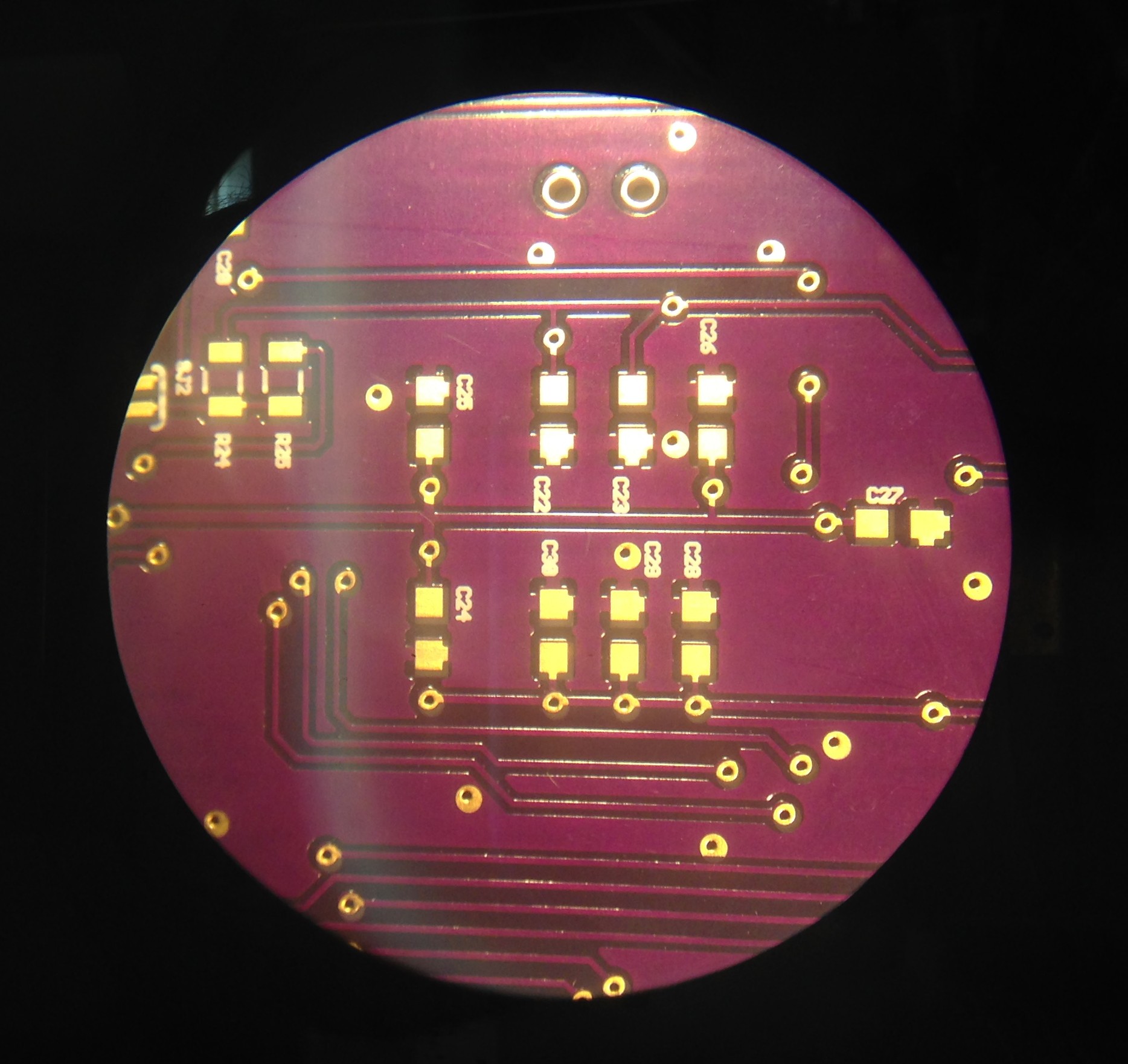
This is a screenshot of the of the layout. The close vias are the ones above C8 and C9 and they are about 9-10 mils from the adjacent trace. I try to space components apart from pads and traces by at least 10 mils. Had I located the vias any closer and there may have been a short. OSH Park’s design rules dictate that the spacing should be at least 6 mil. Of course, one shouldn’t really route traces or create component spacings that that test the minimums. I’m not too sure how the pad got so close to the trace, it could have been due to some offset or under-etching during the fabrication process or a combination of both.
Final Remarks
Overall, I was less than impressed with the quality of the main board but despite all the bad points that I’ve encountered, I haven’t yet run into a problem after populating the board and running some tests on it. I also haven’t noticed any of the same problems on the seven segment display board. Something may have gone awry in the process of populating everyone else’s boards onto the panel or maybe the fab house had an off-day. I’m not too sure what caused the problems.
Would I order from OSH Park again? Yes. If I were designing boards with BGA packages or boards with RF elements, I would be a bit reluctant to order from them but for simple, non time-critical prototypes, definitely yes.